Thesis Pte Ltd

icon

One thesis

Copyright © 

2025

 Thesis Pte. Ltd. All Rights Reserved

OFFICE

34 Boon Leat Terrace #04-09A Singapore 119866

GET IN TOUCH

One thesis

Copyright © 

2025

 Thesis Pte. Ltd. All Rights Reserved

Categories
News Tech bites

Technology Readiness Level

We develop ideas and build solutions to solve tomorrow’s problems. Often, many come to us with promising ideas in need of technical help to develop their concepts. The challenge with idea development is that innovation initiatives frequently fail, falling short of the idealized goal. Several reasons include a lack of understanding of the steps required for a technology to reach commercialization potential and the productization stage and the lack of a simple, actionable development system or innovation strategy. The path from an idea to a fully matured technology requires several steps and processes and almost always involves prototyping steps. (see What constitutes a prototype). The innovation and development of unproven technologies take time, often entail plenty of trial and error, and almost always require a large capacity for taking risks. It is thus essential that each step concerning the development or design of novel concepts or innovative technologies is closely managed with good decisions and done so in the absence of perfect information. Step-wise, innovation execution is essential to the success of many technological projects.

Introducing the TRL scale The Technology Readiness Level (TRL) scale is a metric for describing the maturity of a technology. The scale was introduced by NASA to assess the maturity of a technology prior to integrating it into a system. It has been gaining momentum in adoption, updated, modified and used by other agencies. Most TRL guidelines are based on a scale of 1 to 9, and overtime TRL coverage has been expanded from technical indicators to include additional dimensions of readiness metrics such as hardware and software readiness, system readiness, manufacturability, and ease of integration and even commercial adoption. Further reference links are cited at the end of this article. TRLs have been defined to provide a common metric by which knowledge of new technology’s maturity might be communicated among various engineers, executives, developers and researchers, and among individuals from different organizations. Therefore, TRLs are not linked to a specific technical discipline. The use of TRLs can also provide a needed foundation for developing and communicating insight into the risks involved in advancing a new system, design and its constituent new technology components, and can also be used as a measure of risk associated with introducing new technologies into existing systems This paper considers the need for a higher TRL category, indicating a proven technology demonstrated through extended operational usage, and we have adopted a 1 to 10 scale to make it easier to understand the levels of technological development. The scale can be applied to every project involving technological development.  

TRLs for Innovation and development Level 1 Observe and Report basic principles

This level encompasses ideas and hypotheses where a known fact or process is proposed for a new application. This TRL commences a transition from scientific research to applied research for the development of new technology. Fundamental investigations and paper studies commence.

glass
Conceptual sketch of a wearable eye-movement tracking system

Level 2 – Applied Research: Formulate technology concept and/or application

At this step in the maturation process, research and development (R&D) is initiated. Practical development actions can then be formulated. Applied research, theory and scientific principles are focused on a specific application area to define the concept and characteristics of the application and specified in a document where functional block diagrams are described clearly. Materials and components are procured at this stage.

device
CAD preliminary 3D designs of technology for visualization at TRL 2

Level 3 – Establish critical function, proof of concept

R&D work has begun. Laboratory studies aim to validate analytical predictions of separate components of the technology. This stage is also known as the “breadboarding stage” where demonstration of technical feasibility produces representative data to achieve critical function and/or characteristic proof of concept.

conect board
Electronics or necessary modules required to demonstrate critical function are done at TRL 3

Level 4 – Laboratory testing of prototype component or process

Here, the designs, development and lab testing of various components are integrated to establish that they will work together to achieve the concept-enabling levels of performance required in the final design. They should also be consistent with the requirements of potential system applications. Thus, system-level component and/or breadboard validation in a laboratory environment will identify potential design issues and corrections can be taken at this step.

device
Several modules/components are integrated together for characteristic testing at TRL 4

Level 5 – Alpha testing of the integrated system

The basic technological components (component level, sub-system level or system level) are integrated together with realistic supporting elements to be tested in a simulated or somewhat realistic environment. This prototype stage closely resembles the eventual system and comprises near-finalized electronics or mechanical designs. For example, a new type of solar photovoltaic controller promising higher efficiencies would, at this level, be used in an actual fabricated small-run prototype unit with actually integrated power supplies, protective enclosures, supporting structures, etc., and tested in a simulated environment for data-collection and performance evaluation.

Level 6 – Verify prototype system, begin field testing.

The prototype system is tested and demonstrated in a relevant operational environment where full-scale realistic problems will be observed. If problems arise at this stage, the design must return to TRL 5 or 4 for corrective measures depending on the severity. Engineering feasibility must be fully demonstrated in the actual system application as the design is effectively “locked-in” at this stage and optimized for manufacturability. Ready-to-manufacture (RTM) designs and documentation steps will be carried out to ensure the design is reproducible with the relevant manufacturing steps. Not all technologies will undergo a TRL 6 demonstration. At this point, the maturation step is driven more by assuring management confidence, than by R&D requirements. The demonstration might represent an actual system application, or it might be like the planned application, but using the same technologies.  

Level 7 – Demonstrate integrated pilot system, start tooling and manufacturing.

The prototype is near or at the planned operational system level. The final design is virtually complete. The goal of this stage is to remove engineering and manufacturing risks. The system prototype is demonstrated in an operational environment. In this case, the prototype should be near or at the scale of the planned operational system and the demonstration must take place in the actual field environment. This level of maturity indicates system-engineering and development-management confidence. Not all technologies in all systems will go to this level. For example, solar-powered experimental weather nodes for data-gathering are deployed for extended periods of time to gather environmental data but are not slated for mass production or productization.

Level 8 – Incorporate system in commercial design

The technology has been proven to work in its final form under the expected conditions. In most cases, this level represents the end of true system development. The actual system is completed and qualified through tests and demonstration and is submitted for regulatory approvals at this stage. All commercial technologies being applied in actual systems go through TRL 8. In almost all cases, this level is the end of true “system development” for most technology elements. Most user documentation, training documentation and maintenance documentation are completed. All functionality is tested in simulated and operational scenarios. Verification and validation are completed and commercially launched or deployed en masse.

Level 9 – Deploy the system commercially.

The technology in its final form, thoroughly tested and demonstrated, is ready for commercial deployment. The actual system is proven through successful operations in a variety of conditions across a variety of end-users. In almost all cases, this is the end of “bug fixing” and is no longer considered “technology development”. Successful operational experience and sustaining and/or maintenance engineering support mechanisms are put in place.

car
An example of a TRL 9 is the Tesla Model S sedan vehicle, image credit: Tesla

Level 10 – Commercial Acceptance

The product, process or service has been launched commercially for an extended period, marketed to and adopted by a group of customers (including public authorities). The technology has been used without incident (or with incident levels within an acceptable range) for a protracted period of time. The technology has been certified (if applicable) via appropriate technology-type certification mechanisms, through evaluation of repeated operations and other means. Failure rates for the technology are known and failure conditions and their causes are understood. The technology/system operates without unacceptable levels of unplanned troubleshooting or repair being required.

trl10
Examples of TRL 10 are the Apple iPhone 6 and Boeing 747 aircraft.

TRL summary

An illustration of the TRL scale for increasing technology maturity, in the context of the progression from basic research to system operations.

trltable

Further Reading on TRL definitions

  1. NASA TRL definitions
  2. NASA TRL definitions by John C. Mankins (1995)
  3. John C. Mankins (2009)
  4. ESA TRL handbook
  5. Department of Defense
  6. US department of energy
  7. DoD TRA Deskbook
  8. National Renewable Energy Laboratory– Emerging Technologies in Ocean Kinetic and Enhanced Geo-Thermal
  9. International Standard (ISO) for TRLs known as ISO16290 here.
  10. Jeremy Straub TRL 1-10 discussion paper
  11. European commission “From research to innovation”
Categories
News Tech bites

External Memory for Microcontrollers

Engineers have a wide variety of microcontrollers to choose from for various application needs. While microcontrollers have come a long way with lower power and faster clock speeds – program memory (RAM/ROM) is often still very limited.
There are several reasons for this. First, memory requires a lot of silicon die area. This means that increasing the memory increases the silicon area of the chip and therefore the cost of manufacturing. Second is the issue of the manufacturing process. Different architecture require different manufacturing processes and it is not possible to send different parts of the same chip through different processes.
Since RAM arrays should ideally be optimized in different ways than the rest of the chip, it is more economical to design the memory architecture to match the microcontroller, as a single silicon wafer must be manufactured with the same process to produce individual chips that will be cut out later.
Semiconductor foundries which manufacture RAM chips have dedicated processes for optimizing RAM, not microcontrollers or other logic. Thus, producing RAM on a microcontroller die would mean trade-offs. Since larger RAM arrays have an increased surface area, faults are more likely to develop, simply due to the increased area. This decreases yield and increases costs. If a section within the RAM array on a microcontroller fails, the microcontroller logic must be discarded as well.
The solution is to manufacture microcontroller chips separately from memory chips.
If an embedded system requires more memory to hold firmware, libraries, stacks of persistent data,  a solution is an external flash memory chip, such as EEPROM (Electrically Erasable Programmable Read-Only Memory), serial flash, NOR or FRAM (Ferroelectric RAM) memory chips.
EEPROMs are a standard non-volatile memory, where individual bytes can be independently read, erased and re-written, and they have been dominant on the market for decades. Two other main technologies dominate the non-volatile flash memory market today – NOR and NAND. The newer form of non-volatile memory – FRAM – uses a ferroelectric layer instead of a dielectric layer which enables a higher access speed.
EEPROM memory was invented in 1977 and was the mainstay for microcontroller memory till the NOR flash was introduced by Intel in 1988. The NAND flash architecture was introduced by Toshiba in 1989 and it quickly gained popularity for usage in USB thumb drives, memory cards, compact flash and solid-state memory devices (SSDs).
Let’s look at some options available:

 EEPROMFRAMNOR
Flash
NAND
Flash
SDcard
Flash
Communication interfaceSPI and I2CSPI and I2CMostly SPI/ParallelMostly SPI/ParallelSPI
SpeedDepending on MCU
I2C – up to 1Mhz
SPI – up to 16Mhz
Depending on MCU
I2C – up to 1Mhz
SPI – up to 16Mhz
Depending on MCU
Parallel – 10MHz
SPI – 100MHz
Depending on MCU
Parallel – 10MHz
SPI – 100MHz
Depending on MCU
SPI – 100MHz
Power consumptionLow
~5mA per read/write
Very low
175µA per Read/write
High
~60-100mA
High
~15-30mA
High
~30-100mA per Read/write
Ease of use?EasyEasyRelatively complexRelatively complexRequires FATFS
$ / byte~S$1 / Mbit~S$4 / Mbit~S$8/GbitS$0.5/Gbit<S$1/GB
Typical memory~1Kb – 2Mbit
~(16 – 262 KB)
~1Kbit – 2Mbit
~(16 – 262 KB)
~1Mbit – 2Gbit~256Mbit – 64GbitVery large
Gigabytes+
NoteCan do byte write1 and page writeReal and instantaneous byte read/writeSupports one-byte random accessSequential readSequential read
Write Cycles~1 Million
read-write cycles
100 trillion
read-write cycles
~100k~100k~100k

1mechanism for byte write is based on page write. I.e. an entire page will be written even if just for a byte.
 

Read and Write Considerations

The choice between NOR and NAND depends on your application. NOR reads slightly faster than NAND, while NAND writes much faster than NOR. NAND erases two magnitudes faster than NOR (4msec vs. 5 sec), as most writes must be preceded by an erase operation, while NAND has smaller erase units for fewer erases in less time required. Further details comparing NAND and NOR flash devices are available on a white paper published here, and EETimes has published an article on this topic here.
Which memory type should you choose? NOR is fundamentally a random-access memory device. It has enough address pins to map its entire storage, allowing for easy access to each of its bytes. However, NAND devices require an additional I/O interface or controller, which may vary across models and manufacturers.  NAND is typically accessed in bursts of 512 bytes; i.e., 512 bytes can be read and written at a time, allowing for faster write speeds than NOR. This makes NOR ideal for running code, while NAND is best used as a data storage device (harddrive).
 

Power Consumption Considerations

Depending on your project applications’ needs, you might want to weigh the benefits between ultra-low power consumption and memory capacity. If the project involves wearables with limited battery capacity, or a wireless IoT-type sensor node powered by a solar panel, a low-power EEPROM/FRAM solution might be suitable.
While retaining the same functionality, the advantages FRAM offers over EEPROMs and non-volatile memory are its ultra-low power usage, faster write performance (1,000x faster than EEPROM) and a practically limitless maximum number of write-erase cycles – 100 trillion read/write cycles or greater. To top it off, FRAM is also far more resistant to gamma radiation and electromagnetic fields than other memory types.
However, the disadvantages of FRAM are its much lower storage densities and much higher cost. FRAM memory modules are manufactured by Cypress Semiconductor and Fujitsu as well as Texas Instruments, which is a proponent of FRAM in its MSP430 family of microcontrollers, read more here and here.
 

Choices

How to mitigate reduced storage densities when comparing NAND/NOR vs EEPROMs/FRAMs? The total storage capacity of FRAMs/EEPROMs is daisy-chain upgradable, although this somewhat increases cost at reduced power consumption.
 

 Power Consumption
HighLow
Memory capacityLowEEPROMFRAM
HighFlash memory (SD card / NAND-type)NOR and NAND

Breakouts

 SPI Serial Flash Memory (2Mbits) Breakout
The Winbond’s W25X20CL Serial Flash Memory chip is found in the Xiaomi Miband activity tracker and comes with 2Mbits of non-volatile memory storage. There are 1024 programmable pages of 256 bytes/page via the SPI bus and it boasts a very low power consumption – 1mA (active mode) and 1µA for power down, and operates up to 104Mhz clock speed.
Available from our distribution partner here.
 Cypress FM24N10 FRAM breakout
This has low power consumption (175µA @ 100kHz SCLK read/write operations, 5µA during sleep), high data retention (up to 151 years @ 65℃) and 100 trillion (1014) instantaneous read/write cycles (per byte). It comes in an SOIC8 package and is a direct replacement for most EEPROM parts. Available from our distribution partner here.
 PW163Micron MT25Q 256Mb, 3V, Multiple I/O Serial Flash Memory
The MT25Q is a multiple input/output, 256Mb, 3V, SPI-bus Flash memory device capable of operating up to 133Mhz and it is available in multiple footprints. OEM manufacturer information – MT25QL256ABA

EEPROMs, NORs, NANDs and FRAMs are all commercially available for engineers to select from today. The newest forms of memory, known as MRAM (which is not yet widely available) and NRAM, are set to revolutionize the flash memory market in time to come with applications demanding faster read/write and lower power operations.
Each project and need is unique. To learn more about how we can help you with your design, do contact us.
Build the Future.

Categories
News Tech bites

Introduction to electronic jigs

The final step in an embedded system typically occurs when the firmware or code is flashed into the micro-controller/processor on a PCB and the process almost always requires some sort of physical connection. There are two main methods of momentary contacting assembled electronics – flying probe testing (woodpecker) or a bed-of-nails test fixture.
Both methods involve pins contacting and touching the board on at least two points at a time, allowing for a variety of functional tests to be conducted and/or programmed onto the assembling chips. The difference is that a flying probe utilizes a highly accurate, coordinate-controlled machine head that pans and moves across the PCB testing various points a few pins at a time, whereas a bed-of-nails fixture looks more like an acupressure chair a fakir would use, where dozens to hundreds of pins make contact on the board at the same time.

PCB Design Considerations required

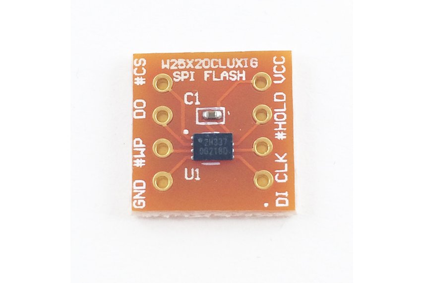
A designer will usually add test pads or programming pads in designs for in-circuit testing with a jig later in the production line.

Flying probe test machines are high-speed, expensive, professional-grade testing equipment generally used for mass-production level PCBs with very fine pitches that don’t have the luxury of test-pad real estate on the PCB. On the other hand, the more common approach will be to use a bed-of-nails test jig if tens of thousands of units are to be programmed or tested.

Test jigs can be built and customized for any type of electronics manufacturing and almost any volume of output, be it mass production or to suit small- to medium-scale electronics manufacturers. Manufacturers of test jigs usually offer both options. SPEA Automatic Test Equipment is one such manufacturer, and configurable kits are commercially available, such as the Merifix PCB test fixture.

Flashing firmware at a prototyping stage

The challenge for designers during the prototyping stage is that it will be too costly to tool a jig for a small run of uncommitted PCB designs and too time-consuming to code coordinates into an expensive flying-probe machine and a conventional approach of adding a connector to each PCB only to remove them later adds unnecessary cost and is wasteful and impractical for loading firmware en masse when the number of test boards increases for various reasons (environmental testing, alpha-user testing etc.)
Enter the electronic test fixture, also known as a jig. Jigs play a crucial role in programming electronics as well as post-assembly testing, also known as in-circuit testing (ICT), where a pogo probe or needle contacts a particular area of the assembled electronics for testing functionality or loading firmware into a chip on the board.
Testing each and every board on the manufacturing line is unavoidable, and in cases where a manufacturer produces tens of thousands of units in a day, timing is critical and automatic test jigs are capable of programming/testing and identifying/removing defective units for rectification or disposal. They can also reduce costs because they allow even non-technical people to perform the tests.

In our labs, we build test electronics on a daily basis, and testing them is just as important. Here we show make test jigs quickly on a small prototyping scale by building a jig resembling a bed-of-nails test fixture using pogo pins for customized, small-volume testing and programming.

With our completed PCB, you can now mirror the PCB design and expose all vias (un-tent) or test pads and fabricate a mirrored PCB of the layout to your specific debugging port pin-layout depending on the chip or microcontroller you may be using.

Actual electronics to be tested/programmed are placed on a mechanical holder of the jig, and the pogo bed-of-nails PCB is then lowered down to make contact with the target electronics. The entire setup will be placed inside a custom-designed 3D-printed jig, with the programming PCB wired out to the debugger interface or a programmer. The spring-loaded (pogo) pins are recommended when placing electronics on a jig and the contact points are temporary and may be uneven.

Actual electronics to be tested/programmed are placed on a mechanical holder of the jig, and the pogo bed-of-nails PCB is then lowered down to make contact with the target electronics. The entire setup will be placed inside a custom-designed 3D-printed jig, with the programming PCB wired out to the debugger interface or a programmer. The spring-loaded (pogo) pins are recommended when placing electronics on a jig and the contact points are temporary and may be uneven.

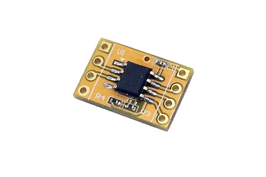
The mechanical structure of the jig is 3D-printed for quick prototyping
The pogo pins are then aligned with a dummy target board and soldered in place. (This step is optional if the design already has a PCB sandwich to align the pogo pins).
The target board is then placed in the mechanical slot designed into the jig, and the programming PCB is then mounted by other 3D-printed parts and – viola the programming-/-test jig is complete.

The various components of a jig are laid out.
There is no hard-and-fast rule in a jig design. For alignment, the programming pogo-pin interface can be sandwiched between 3D-printed parts, or two PCBs can be used for alignment. Pogo pins can be downward- or upward-facing, depending on where the test pads are or which approach is more convenient.
Another angle shows the use of two PCBs to align the pogo pins, with the pogo pins upward facing.

A 3D prototype of a jig can be designed and printed in a day, and all minor-dimension tweaks can be done right at your desk. You’ll be ready to test and program small batches of target projects quickly, painlessly and effectively. Program-test-pass, place the next target board in the jig, run the program, and so on and so forth.

One of our rapidly-prototyped jig setups connected to a programmer.
We hope you find this entry useful, do talk to our consultants to learn more about our range of services which include full turnkey design, electronics, hardware, software and full-stack firmware design.

Build the Future!

Categories
News Tech bites

We need more USB ports


In the pursuit of ever-slimmer laptops, manufacturers are removing what appears to be “bulky” USB ports from their new product releases. That may result in a slimmer notebook, but more often than not, individuals end up adding dongles and further bulk so that existing peripherals can still be used.

Mobile developers on our team use the Microsoft Surface Pro 3, and it has been a great laptop for mobile development since most of our software development kits (SDK) and integrated development environment (IDE) run on Windows. It’s compact, feels good, is light (only 800g!), has a touchscreen, and sports a beefy Intel Core i7-4650U processor. It’s perfect. Except for one thing.

It has only one USB port.

Although the single USB port is not yet a widespread design adoption with Windows-based laptop manufacturers, the net was abuzz with gripes surrounding Apple’s design of a single USB-C port on its new range of MacBooks. CNET published an article on some “survival tips”, but it doesn’t hide the fact that sometimes we do need more ports on our computing devices – development kits, Universal asynchronous receiver/transmitters (UART), USB-to-Serial, Bluetooth4.1 dongles, syncing our smartphones and other memory devices. You name it.

A USB hub is an obvious solution. But somehow none of the USB hubs we’ve tried has had the right combination of data-transfer reliability and aesthetics. Cheap hubs with the right profile keep disconnecting our devices, while reliable hubs are expensive.

Is it too hard to ask for a few more USB ports? So we made our own.

Selection of a hub-controller chip is easy, as just about practically every semiconductor manufacturer has a product line of USB hub controllers. Texas Instruments, STMicroelectronics, Cypress, Maxim, Renesas, so on and so forth. Each manufacturer has slight peripheral advantages in its chips over its competitors.

However, a key goal was to keep costs low, which is a good design practice to determine the cost of your Bill of Materials (BOM) before jumping into the design. More often than not, engineers/inventors jump straight into a design and realize far too late that the costs of constructing that particular design reduce the value proposition of the invention or device they are trying to make with marginal improvements over existing solutions.

Consumers are more well-informed when it comes to the selection of products and devices pertaining to their technological tastes and needs, where cost and value are no doubt factors in a decision to purchase.

A quick cursory search revealed Chinese and Taiwanese semiconductor companies producing equivalent USB hub controller chips. Such as Alcor Micro, Genesys Logic, and JFD-IC, FE1.1s which are likely producing the bulk of the world’s original-equipment-manufacturer (OEM) USB-controller chips.

We found Genesys Logic’s GL850G controller chip in one of the hubs lying around the lab. Alcor Micro’s AU6256 and JFD-IC’s FE1.1s also presented attractive options.

As a designer, several factors should be considered.

  1. Does your manufacturer have access to the components that require assembly?
    If it does not, it’s likely that you will have to set up that relationship.
  2. Can you get the necessary components in the volume that you require?
    It’s unlikely that you’ll get 10 pieces from an OEM manufacturer if you cannot commit to a Minimum Order Quantity (MOQ) or sales volume, otherwise you might have to get a more readily available component from a distributor like Future Electronics, Arrow Electronics, Avnet, Digikey, Element14 or Mouser.
  3. Is there a commercial relationship between you and the component provider?
    More often than not, OEM manufacturers from China, Taiwan or South Korea converse in their native languages and cross-border sales teams will face challenges in currency conversions, customs restrictions and/or taxes, and the offset of these hidden costs may render the component more expensive to implement in your design than originally anticipated.

Availability, MOQ, documentation, and cost-per-chip are all factors an engineer has to be aware of during the process of a design. In the end, we selected Standard Microsystems Corporation (SMSC)’s USB2514 USB 2.0 Hi-Speed Hub Controller. SMSC is now owned by Microchip, which means the chip is marketed by a reliable and reputable OEM semiconductor company with established distribution channels.

The USB2514 had a good price of US$1.40 a chip, comprehensive documentation, very minimal BOM and, most importantly, is widely available and accessible to electronic contract manufacturers and assemblers.

Here is our design and the final outcome!

Top view (male USB headers were soldered on later)

Male headers were soldered, and heatsinked for protection and then distributed to our engineers

Close up
In our opinion, it looks more badass-punkish when its bare electronic guts are exposed. Future design iterations would involve changing the hub to a USB-3.0 controller and possibly include other mechanical features or enclosures; for now, this design works fine and is a talking point when our mobile engineers assist clients on-site. Check out our USB-C “spacedock” design for advanced features that were later added. If you’re interested in making such of a USB hub of your own, we would love to work with you.
Build the future!

Categories
News Tech bites

Intro to Eddystone – Google latest proximity beacon protocol

During the height of iBeacon, google released a similar and more powerful proximity beacon protocol called EddystoneTM in July 2015. The protocol was designed to be platform agnostic and more flexible in the data that can be broadcast. The key features were designed to make it a better platform than the iBeacon protocol. App developers can find more information on the available API here.

However flexible google wishes to design the EddystoneTM to be, they have to keep in mind the space limit of a BLE broadcasting data. Instead of trying to cram all sort of data within the data limit, google overcame the problem by introducing “frames”. A total of 3 different data frames was designed into the EddystoneTM protocol- namely UID, ULR and TLM. Each frame was designed to carry different set of information to fulfill the broadcasting need of most proximity beacon.

UID

The most basic of the EddystoneTM protocol with frame specification that is very similar to the iBeacon’s. In this frame, user will have to indicate the unique ID of the device, the instance ID and the transmission power.  The unique ID is also known as namespace, which is a 10bytes data. User can generate it using an online UUID generator. The instance ID works the same as the Major and Minor ID from iBeacon. Finally, the transmission power, aka ranging data. To calibrate this – “Tx power is the received power at 0 meters measured in dBm. The value may range from -100 dBm to +20 dBm at a resolution of 1 dBm (source)

Note to developers: the best way to determine the precise value to put into this field is to measure the actual output of your beacon from 1 meter away and then add 41 dBm to that. 41dBm is the signal loss that occurs over 1 meter.”

Unlike the iBeacon’s transmission power which was supposed to be measured at 1m range, EddystoneTM requires the transmission power to be measured at 0m instead. However, noting from the calibration information provided by google, the transmission is supposed to be measured at 1m range and you add 41dBm to account for the signal loss over 1 meter. The result is the transmission power at 0m.

URL

This frame is designed to house an URL for your proximity beacon to broadcast. Do make sure to indicate “0x10” in the Frame Type byte, else the EddystoneTM APP API will not recognize the frame properly. Following that is the transmission power, which can be calibrated with the same procedure provided in the above section. The URL scheme indicate which html prefix to be appended to the decoded URL and currently, there are 4 options to choose from:

Finally, it’s the encoded URL. For example, if I wish to broadcast “onethesis.com”, my encoded URL will looks like “0x6f6e6574686573697300” (with padding: onethesis = 6f 6e 65 74 68 65 73 69 73), note that the data is entirely in hexidecimal). The string is ended with the URL with “0x00” which will be decoded as “.com/”. A full list of the ending character is listed below:

TLM

This frame is also known as the telemetry frame. It holds device specific information which could be useful for debugging or data-logging purpose. To start with, user must indicates “0x20” in the Frame type and followed by the TLM version. The subsequent data are device specific information like battery voltage, Beacon temperature, Advertising PDU count (ADV_CNT) and Time since power-on or reboot (SEC_CNT).

Battery voltage is in 1mV per bit resolution. Beacon temperature is in degrees Celsius expressed in 8.8 fixed point representation. ADV_CNT counts the number of advertising frame that has been sent since power-on or reboot. SEC_CNT is a 0.1 second resolution counter. It is not necessary to provide all of the data. User can choose to obscure certain data by simply not updating the values.

One important note about this frame is that it cannot be a standalone frame in the EddystoneTM protocol. It should always be used in conjunction with the UID or URL frame.

Resources

As usual, for firmware developer, Cypress Ez-BLE pioneer kit provides easy access to learning this protocol and Cypress has provided some examples for their users as well (source).

Build the Future

Categories
News Tech bites

Understanding Ethernet Cables

It binds us. It connects us. It gives us knowledge. It’s omnipresent and omniscient. It’s… Wi-Fi.

Well.  Sometimes we forget that Wi-Fi signals and connectivity still require a much underappreciated and most needed component –


The Ethernet cable.

Your mobile connectivity has to come from some sort of wireless hub, which is connected to either an Ethernet or fibre-optic cable these days. For this post, we’re looking at the standard Ethernet cable used for VoIP phones, routers, switches, hubs, servers, computers, network printers and more. To the casual user, these cables come in a confusing array of choices.

However, there is, in fact, a difference between all those network cables. They look and any of them will plug into an Ethernet port, but they do have some differences on the inside.

So let’s say you need to get some new cable to setup a small home network, and you walk into a gadget store and say “Hi, I’d like to get some computer cable”.

That’s not going to be helpful. The differences between each type of cable are due to various network standards. Here’s what you need to know about how they’ll affect the speed of your home or work network:

Cat5 – Oldest type and slowest – Category 5 cabling, also known as Cat5, was made to support theoretical speeds of 10-100Mbps (10BASE-T, 100BASE-TX). Since Cat5 is an older type of cabling, you probably won’t see it much in stores, but you may have gotten some with an older router or another networking device. Most Cat5 cables are unshielded, relying on the balanced line twisted pair design and differential signaling for noise rejection. Cat5 has been superseded by the CAT5e (enhanced) specification.

Cat5e – Faster with less interference – Category 5 enhanced cabling is an improvement on Cat5 cabling. It was made to support up to 1000 Mbps gigabit speeds, so in theory, it’s faster than Cat5. It also cuts down on crosstalk, which is the interference you can sometimes get between wires inside the cable. Both of these improvements mean you’re more likely to get a faster, more reliable speed out of Cat5e cabling compared with Cat5. This is the most common cable that is in use today.

More details of a Cat5e cable’s specifications can found here.

Cat6 – Consistent gigabit speeds – Category 6 cabling is the next step up from Cat5e, and includes a few more improvements. It has even stricter specifications when it comes to interference, and is even capable of 10-Gigabit speeds.

It’s used in large networks, small data centers and in a business environment. You probably won’t use these speeds at home, and the extra interference improvements won’t make a huge difference in regular usage, but if you’re purchasing a new cable, you might want to consider Cat6 for future upgradability.

One thing to note with extra shielding, Cat6 cables are slightly thicker and slightly less pliant, meaning they won’t bend around corners or coil as easily as compared with Cat5 cables.

Cat 6a (Augmented) – Server-type cables – These cables are the fastest and most expensive cables available for the highest consistent speeds in server farms, network servers and distributed / parallel computing applications.

All cables are backward compatible, meaning the higher categories can work with the lower categories of Ethernet. An interesting thing to note is that there are other categories of cable, Cat7-8, but they are not recognized by the TIA/EIA and few manufacturers make them.

So Which Should You Use?

It’s important to note that your network speed is different than your internet speed. Chances are, upgrading your cables isn’t going to make a difference in how fast you load that YouTube video. Your ISP speeds are likely to be much slower than your network. But if you are transferring files between computers (i.e. you’re backing up to a NAS) or streaming videos, then using gigabit-compatible hardware will speed up access time, but your router and computer ports should be gigabit-compatible as well, otherwise, the bottle neck is just shifted elsewhere. Also, if you’re running cable throughout your house, you may notice a decrease in speeds if you are using cables longer than 100 meters.

What type of cable are you using?

The printed text on the cable will usually give you some clues. In this example, the similar color arrangement of the cable tells us that the cable is a straight cable.

Straight and crossover cables are wired differently from each other. One way to tell what you have is to look at the order of the coloured wires inside the plastic RJ-45 housing. The RJ-45 connector is the standard type connector used for Ethernet connections compared with the smaller RJ-11 connections used on telephone cords. Crossover cables are less common and are used in computer-to-computer applications. The more common cable will be a straight cable, where you connect a network device (say a router) to your computer or wireless-access points.

What you can do is put both ends of the cable side by side with the connector facing the same way and see if the order of the wires is the same on both ends. If so, then you have a straight cable. If not, then it’s most likely a crossover cable or was wired wrong.

Our cable reads “CAT5E” “TIA/EIA568B” “4STP” “24AWG”, what it means:

  • Cat5e Category 5 Enhanced cable
  • TIA/EIA568B means this cable is compliant to the standards set by Telecommunications Industry Association (TIA) of the Electronic Industries Alliance (EIA) for commercial building cabling, pin/pair assignments for eight-conductor 100-ohm balanced twisted pair cabling. These assignments are named T568B, the latest version is T568C as of 2014, more of this standard here.
  • 4STP means four cables of S = braided shielding (outer layer only), TP = twisted pair. This is a four-wire shielded twisted pair (STP) of wires, more can be read on Ethernet cable construction here.
  • 24AWG denotes how thick the copper wires of the cable are. American wire gauge (AWG) is a standardized gauge system for indicating the diameter of conducting electrical wire and is commonly used among electrical engineers. The rating gives information regarding the resistance of the wire and the allowable current (ampacity) based on plastic insulation. In this case, 24 represents as cross-sectional diameter of 0.51054mm (0.205 mm2) and a copper resistance of 84.22mΩ/m (0.842Ω/metre), which is a typical impedance of 100 ± 15Ω.

Cable health

Ok, now you know a whole lot more about Ethernet cables, you fish out one from the rat’s nest where you’ve stored all the random cables in your house, you find the Ethernet cable and plug it in.

It doesn’t work.

Great, what now? How do you tell if it’s a bad cable?

Wouldn’t it be great to know if the wires inside the cable had broken? Especially if it’s an expensive Cat6 type cable or if the cable is especially long.

We got an RJ-45 network cable tester from Amazon, however, this little gadget isn’t intuitive at all. According to the poorly written manual, the lights will turn on sequentially from 1 to 8 if the tested cable if fully functional. It works sporadically and basically, gives an “OK/NOT OK” binary output by means of a single LED.

Next, we got ourselves RJ-45 punch-down blocks from Amazon, and they were a pain. The clips required pliers to remove and more wires needed to be punched in the teeth before any sort of testing could be done. A real inconvenience.

There must be a better way – so we created a new solution. The easy-to-use RJ-45 Ethernet cable tester for a quick, low-cost, painless way to test your Ethernet cables.

This is as simple as it gets – two RJ-45 receptacles. Plug in your Ethernet cable and use a continuity checker or a Multimeter and you will know if your cable works or is broken.

You can now test the resistances of each point in your cable using your Multi-meter and determine if your cable meets the necessary tolerances. Typical Cat5e cables have a 10ohm/100m conductor resistance, resulting in a 1ohm/10m loop resistance, with tolerances included, you should measure an end-to-end wire resistance of <20 ohms per 100m length, or about 0.2Ω/metre.

Or you could simply do a continuity test to ensure your cables aren’t broken or if there are missing wires. We tested all our Cat5/Cat5e cables, flat, shielded, long and short, in seconds! This nifty gadget was born out of frustration in finding a simple, low-cost means of testing lots of Ethernet cables quickly and easily and our engineers now use it frequently. It’s a must-have for any engineer/technician working with lots of Ethernet cables.

If you liked this post, subscribe with your email below, and we’d love to hear from you, also we’ll be happy to hear suggestions and comments for improvement in the comments section below.

Build the future.