Thesis Pte Ltd

icon

One thesis

Copyright © 

2025

 Thesis Pte. Ltd. All Rights Reserved

OFFICE

34 Boon Leat Terrace #04-09A Singapore 119866

GET IN TOUCH

One thesis

Copyright © 

2025

 Thesis Pte. Ltd. All Rights Reserved

Categories
News Tutorials

How to create an LTspice model from PSpice or Tina-TI model?

LTspice is a SPICE-based analogue electronic circuit simulator computer software produced by semiconductor manufacturer Analog Devices (originally by Linear Technology).[1] It is the most widely distributed and used SPICE software in the industry.[2] Although LTspice is a great free-to-use SPICE software with many built-in models, the models are either generic models or Analog Devices specific components. You will need to import other manufacturers’ models into LTspice. In this post, I will discuss the import of the TINA-TI or PSpice model. If the model contains “SUBCKT”, you can easily do it. 

Importing from PSpice

This import method is the easiest. Let’s follow the following steps:

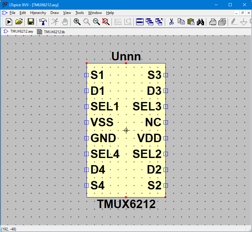
  1. Download the PSpice model from the manufacturer’s website. For this post, I will use TMUX6212 as an example.
  2. You will find a few files in the model compress file, but the only file of interest here is a .lib file. In this case, it is TMUX6212.lib.
  3. Open that file in LTspice.
  4. Highlight the component name besides “.SUBCKT”.
  5. Right-click and select “Create Symbol”.
  6. Click Yes.
  7. LTSpice will auto-generate the symbol with a “.asy” extension into the auto-generated folder of LTspice (C:\Users\user\Documents\LTspiceXVII\lib\sym\AutoGenerated). Take note that the path depends on your settings.
  8. You can feel free to re-arrange the symbol and save it.
  9. You can add the symbol from the component library to your schematic. Please test the model before using it. In my example, you can conduct simple tests like whether the logic, switching, and power rails work. You can also go deeper to test resistance and bandwidth. I will not discuss the testing method in this post.

Importing from TINA-TI

Before you begin, you need to ensure you have installed TINA-TI. If you have, you may proceed.

  1. A component page usually comes with a TINA-TI simulation reference design schematic to download. In my case, I will use MUX36D04 as an example.
  2. Downloading the reference design will give you “sbom969a.tsc”.
  3. Open that file in TINA-TI.
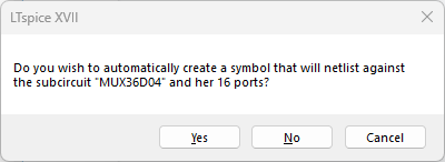
  4. Right-click on the model and select “Enter Macro”.
  5. This action will open the macro file. Now perform a “Save As”, and this will create a .cir file.
  6. Open the .cir file in LTspice.
  7. Highlight the component name besides “.SUBCKT” and right-click. Then select “Create Symbol”.
  8. Click YES
  9. LTSpice will auto-generate the symbol with a “.asy” extension into the auto-generated folder of LTspice (C:\Users\user\Documents\LTspiceXVII\lib\sym\AutoGenerated). Take note that the path depends on your settings.
  10. You can feel free to re-arrange the symbol and save it.
  11. You can add the symbol from the component library to your schematic. Please test the model before using it. In my example, you can conduct simple tests like whether the logic, switching, and power rails work. You can also go deeper to test resistance and bandwidth. I will not discuss the testing method in this post.

How to make the model portable?

Occasionally, you want the imported model to be portable so that you can share the simulation schematic.

  1. Follow the above import instruction for either PSpice or TINA-TI.
  2. Go to the AutoGenerated folder and open the symbol file using a text editor.
  3. Remove the absolute path of the model file. I will modify the following line to “SYMATTR ModelFile TMUX6212.lib” in my example.
    1. This will change the symbol to read from the lib file within the same folder.
  4. Copy the model file into the same folder as the symbol. The model file can be either a .lib file or a .cir file, depending on where you import from.
  5. To use this symbol in your schematic, you need to place the schematic, symbol and model file into the same folder because the LTspice component select dialogue only shows two directories by default – your schematic directory and the installation component library directory.

I hope you will find this post useful in your simulation journey.


Kickstart Your Product Idea
As your strategic product partner, THESIS is always ready to help you innovate and value-add on your products.

Contact us:
contact@onethesis.com
www.onethesis.com
www.linkedin.com/company/onethesis
www.twitter.com/onethesistech
www.instagram.com/onethesis/


[1]  “LTspice”. Analog Devices. Archived from the original on December 3, 2018.

[2]  “LTspice XVII Introduction”. LTwiki. Archived from the original on December 2, 2018.

Categories
News Tutorials

Gerbers to Footprint!

Foreword

This post is excellent for those who are looking to extract reference designs (in Gerber files) from silicon manufacturers. In this example, I am trying to save myself from having to draw a PCB trace antenna from scratch! We will copy the reference antenna design from Dialog Semiconductors for its DA14580 BLE chips and use that as a footprint for my PCB.

Let me show you how to extract a component footprint from the Gerber files,

Tools

Gerber Files

In this example, I downloaded the reference PCB trace antenna design from Dialog and extracted the Gerber files which were in ART format. These are the “blueprints”, if you will, to a PCB manufacturer in terms of how each layer of the PCB is supposed to look.

PCB Design Software

We will be using Altium Designer 13.1 PCB Design software for this tutorial.

Reverse Engineering the Gerber Files

Import Gerber and Drill Files

First, we have to import the Gerber files into Altium Designer. Create a new CAMtastic document by clicking File>New>CAM Document. Next, initiate the import process by clicking File>Import>Gerber.

 
Select the desired Gerber files (i.e. layers of interest) into the CAMtastic document.
 
TIP: Click on “Settings…”.
 
TIP: Follow the above settings.

It is important that you follow the recommended settings during the import. This will guarantee that the dimensions are correct (in my first few attempts, they were several times larger). Now click “OK” to execute the import.

The imported Gerber files. Highlighted here is just the Top layer which I am interested in.

The import process is not complete yet without the Drill file(s). Initiate it by clicking File>Import>Drill. Follow the same import settings as with the Gerber files. TIP: If we don’t import the Drill files, we won’t be able to extract the netlist(s) later on to export to PCB.

 
Select the Drill file(s) to load into the CAMtastic document.
 
TIP: Select the appropriate import settings.

Providing Information about the Layers

To extract the netlists, we need to first associate and establish the layer sets (for eg. the drill layer and top and bottom layers). Click on Tables>Layers Sets. You need at least ONE layers set to move on. You should also set the Layers Order by clicking Tables>Layers Order, otherwise, you will encounter an error when trying to export to PCB.

 
Insert a layer set by associating the drill layer(s) with the signal/plane layer(s).

Extract the Netlists

We need to now extract the net(s) by clicking on Tools>Netlist>Extract. Now, the traces are identified with a net as they were during the PCB design process.

 
TIP: Ensure the netlist(s) are extracted from the Gerber files. You can export it to a PCB document.

Export to PCB Document

To generate the PCB document, click on File>Export>Export to PCB (previously grayed out if the preceding steps are not performed). You will now see all the Gerber files being converted into the PCB document.

 
TIP: Select the desired trace(s) that you want to copy as a footprint.

Copy as Footprint

After you have selected the trace(s) that you wish to copy, paste them in the Footprint PCB Library and create a new component for it.

 
Now you’re ready to rock and roll with your new footprint reference design!

Summary

We have gone through a step-by-step analysis on how to import the reference design in Gerber files, extract the necessary layer and netlist information, convert them into the PCB document and thereafter be able to reuse it as a component footprint! Perhaps, if you had tried to draw this from scratch, you would have taken a full day to do just that.

I hope that you found my example useful and hope it will come in handy for any advanced users out there. Thanks for reading!

References

  1. https://techdocs.altium.com/display/ADOH/CAM+Editor+Reverse+Engineering+PCBs
  2. https://techdocs.altium.com/display/ADOH/CAM+Editor+Panels+for+Fabrication+and+Assembly
  3. http://techdocs.altium.com/display/ADOH/CAM+Editor+Data+Verification